
20.1 Why semiconductors matter
A semiconductor is a chip: a piece of silicon carrying billions of microscopic switches that do arithmetic, store data and control machines. Chips run phones, cars, hospitals, factories, power grids and weapons. When they stop arriving, whole industries stall. The shortages of 2021 and 2022 idled car plants around the world, and that episode is a large part of why governments began treating chip-making as strategic infrastructure.
Most countries buy chips and build nothing. Only Taiwan, South Korea, the United States, Japan and parts of Europe and China manufacture the most valuable ones at scale. India has long designed chips and exported software, but it has manufactured very few. Fabrication, the step where designs become physical silicon, was the missing layer. A fab in India is therefore less a factory story and more a question of whether a whole industrial capability can be built from close to zero.
20.2 The Tata semiconductor project
The words need unpacking first. A fab (short for fabrication plant) is the facility where chips are printed onto wafers. A foundry is a fab that manufactures chips designed by other companies, rather than only its own; the Dholera facility is planned as a foundry, which means its output serves whoever contracts for capacity. Fabrication sits between design (done on computers, largely in India already) and assembly, test and packaging (covered in section 20.8). Each stage is its own industry, with its own economics.
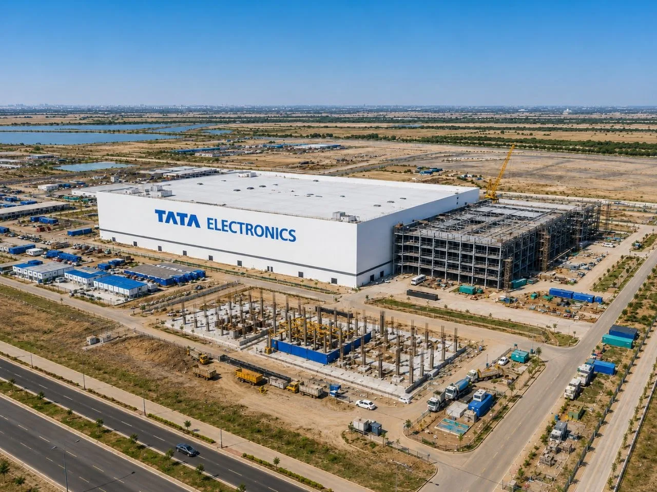
The anchor of Dholera's semiconductor story is a fab being developed by Tata Electronics in partnership with Powerchip Semiconductor Manufacturing Corporation (PSMC) of Taiwan. The project was approved on 29 February 2024 under the India Semiconductor Mission (covered in the timeline chapter). The partnership matters because PSMC brings proven process technology; Tata brings capital, project management and India-scale execution.
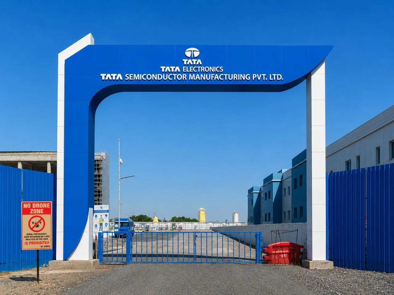
The approvals that followed in September 2024 turned the sanction into a working programme: the India Semiconductor Mission, Tata Electronics and Tata Semiconductor Manufacturing signed a fiscal support agreement formalising government financial backing for the project, Tata Electronics and PSMC signed the definitive technology transfer agreement covering process technology, engineering support and operational know-how — a prerequisite for detailed design and equipment procurement — and the fab was formally notified at the Dholera SEZ, enabling customs and duty benefits.
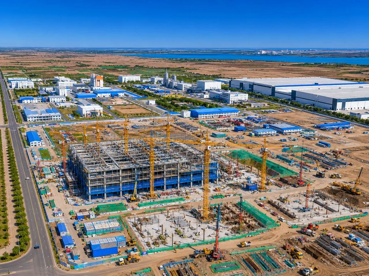
The project sits inside a notified Special Economic Zone. A government SEZ notification dated 9 April 2026 records the Dholera unit at 66.166 hectares, with a proposed investment of ₹91,000 crore and proposed employment of 21,000. Those are notified proposal figures, not outcomes; a notification records what is proposed, not what has been built.
A date has also been put on the outcome everyone is waiting for. In September 2026, Union IT Minister Ashwini Vaishnaw said India's first semiconductor wafer is likely to roll out of the Dholera plant in 2028, and Tata Electronics CEO Randhir Thakur confirmed at SEMICON India 2026 that the fab remains on track, with tool installation targeted for late 2027. The full dated chain is recorded in the intelligence entry on the 2028 first-wafer target.
The fab is under construction. For the current construction picture and anything recent, see Dholera Ground Reality (Chapter 6) and the news record; this chapter sticks to what the project is and what it demands, not day-to-day progress.
20.3 Semiconductor manufacturing
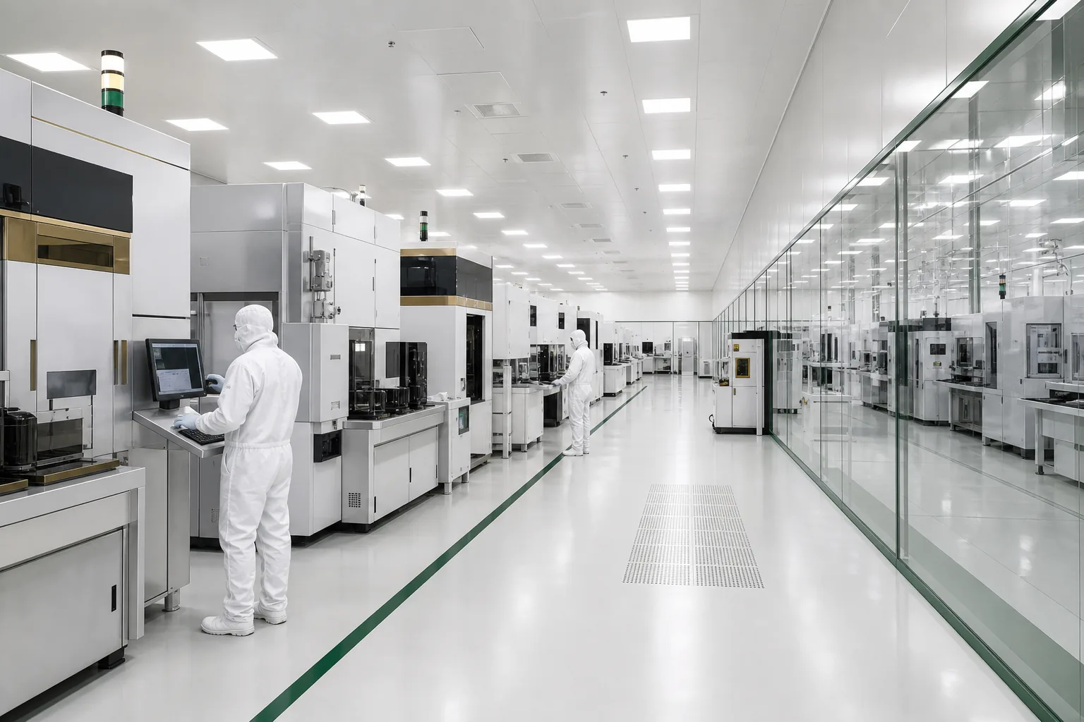
A fab does not assemble chips like a factory assembling cars. It grows and prints them, layer by layer, on thin discs of silicon called wafers. Each wafer passes through hundreds of steps: polishing, coating with light-sensitive material, exposing patterns through lithography machines, etching, depositing metals, and testing. A single wafer can take months to travel through the line, and a dust particle the size of a virus can ruin the die it lands on.
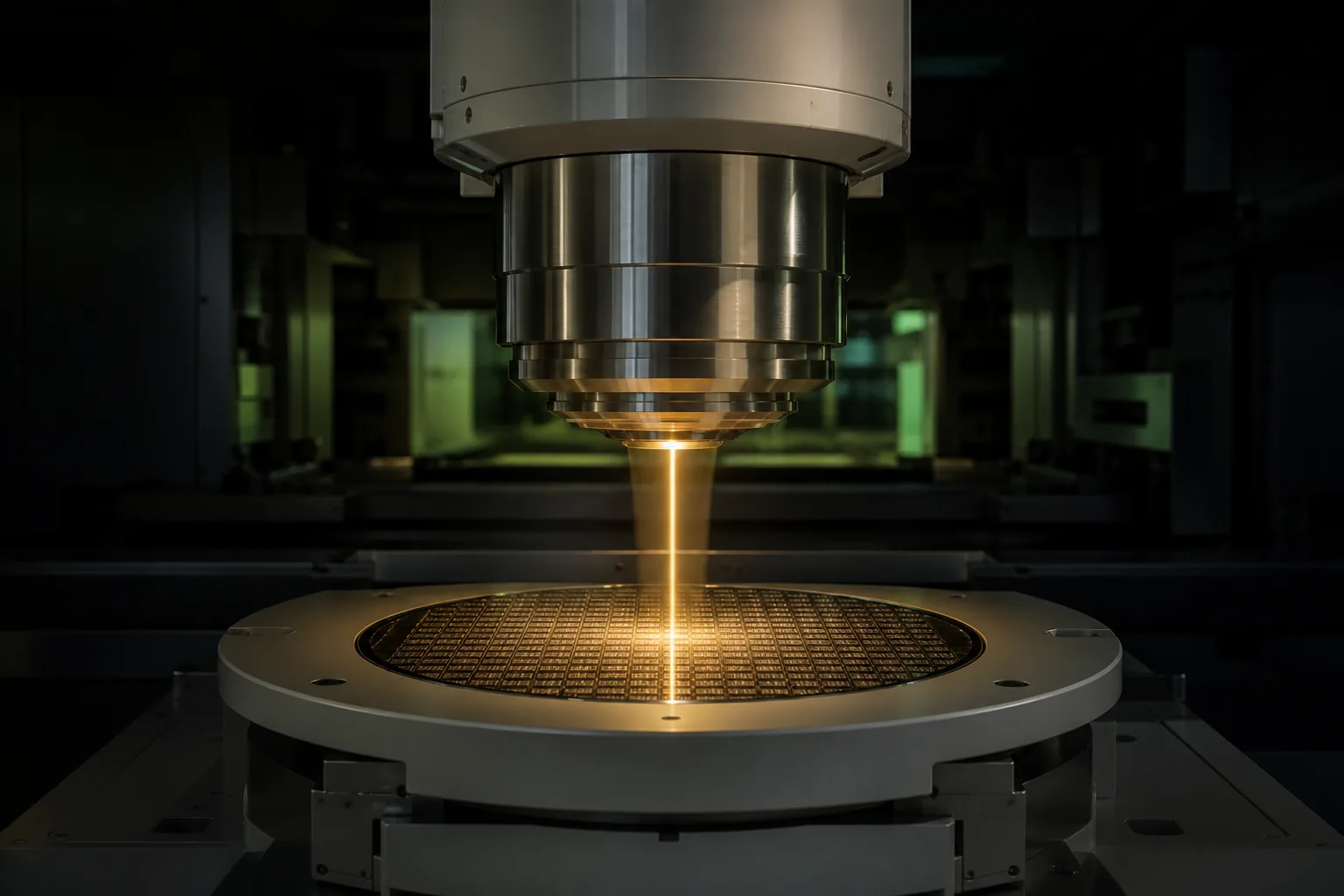
The Dholera fab is planned around mature process nodes: technologies in the 28 to 110 nanometre range, according to Tata's foundry page. "Mature" does not mean obsolete. These nodes power the chips the world actually runs short of: power management ICs, display drivers, microcontrollers and similar workhorse chips used in cars, appliances, industrial equipment and telecom gear. Newer, smaller nodes suit phones and AI accelerators; mature nodes suit everything with a plug or a battery. The world's shortage problems have clustered here.
This is also a deliberate sequencing choice. Building a leading-edge fab before a country has any fab experience is extremely risky. Mature-node manufacturing lets engineers, suppliers and operators learn on demanding but established processes first.
The design capacity, per Tata's foundry page, is up to 50,000 wafer starts per month. "Wafer starts" is the industry's way of counting: one wafer entering the production line, whatever happens to it afterwards. At that scale, one fab would produce a meaningful share of the mature-node chips India currently imports for its cars, appliances and telecom networks, though capacity on paper and capacity in production are separated by years of learning, a distinction the status chapters track.
20.4 Fab requirements
What a fab needs goes far beyond land and a building:
A cleanroom shell
Manufacturing happens in spaces where air is exchanged and filtered many times per minute, far cleaner than a hospital operating theatre. The building is effectively a machine itself.
Ultra-pure materials
Silicon wafers, photoresists, etching gases and specialty chemicals all arrive at purities measured in parts per billion. Ordinary industrial-grade inputs would ruin production.
Precision equipment
Lithography, deposition and etching tools cost millions of dollars each, come from a small number of suppliers, and require installation, calibration and maintenance at factory grade.
Process discipline
Thousands of steps must repeat identically for months. Yield, the share of good chips per wafer, is the whole business, and it is built on measurement, data and operator training.
These requirements explain why so few countries make chips. The knowledge is not in one machine; it is distributed across the building, the utilities, the suppliers and the people.
20.5 Utilities required by fabs
A fab consumes utilities at a scale closer to a small city block than a factory. Continuous supplies of clean, stable power run the tools; chilled water and clean dry air hold the cleanroom's temperature and humidity within fractions of a degree and a few percentage points; process cooling, vacuum and compressed gases run through dedicated networks in the ceiling and under the floor.
The critical property is not volume alone but quality and continuity. A half-second voltage dip can scrap wafers mid-process, so fabs install uninterruptible power, on-site generation backup, and power conditioning on top of the grid supply. This is why a fab location is judged as much on grid reliability as on tariff.
Chemical and gas delivery systems, waste collection for acids and solvents, and exhaust scrubbing round out the picture. Every input has a matching, regulated output path. The regional water and power picture is covered in Infrastructure — Water and Infrastructure — Energy.
It is worth seeing how unusual this utility profile is. A typical factory buys power, uses it roughly, and shuts down at night. A fab buys conditioned power, uses it continuously, and treats every microsecond of disturbance as a quality event. Its air, water and gas systems are engineered to tolerances closer to a laboratory than a workshop, and they run 24 hours a day for decades. That is why fabs are described as among the most complex industrial facilities ever built. The complexity is not in one machine but in the machine-plus-building-plus-utilities as a single system.
20.6 Water and power requirements
Water deserves its own section because the numbers surprise people. Wafer rinsing and cleanroom systems use ultra-pure water; ordinary drinking water is far too contaminated, so the fab runs its own treatment chain that strips out minerals, organics, bacteria and dissolved gases. Producing one litre of ultra-pure water takes more than one litre of raw water, and a large fab can use millions of litres a day. Recycling rates matter enormously, and wastewater from etching and cleaning needs treatment before anything is discharged.
Power follows the same logic of quality plus scale. A mature-node fab drawing tens of megawatts continuously needs a grid that does not flicker, plus backup for the moments the grid does. This is where Dholera's planned infrastructure becomes relevant: the region's power arrangements, renewable capacity and water systems were designed for exactly this class of industrial tenant. What has actually been commissioned, and to what extent, is tracked in Chapter 6, not here.
20.7 Supply chain
No fab is self-sufficient. It depends on a continuous flow of silicon wafers, photoresists, specialty gases, acids and solvents, spare parts for precision tools, and technicians who can keep that equipment running. Many of these inputs have few suppliers worldwide, and some are sourced from a single country. A missed chemical shipment can idle a production line just as effectively as a power cut.
This is why fab locations get judged on logistics and supplier proximity as much as on land price. Partnerships around the Dholera project point the same direction: Tata announced a partnership with ASML, the Dutch lithography-equipment maker, on 17 May 2026, and equipment and design ties to suppliers such as Tokyo Electron and Synopsys have been reported in company and press records. Each such tie is a supply-chain dependency made visible; it is also an ecosystem signal.
Two recent items show how the operational side of the supply chain is being contracted into existence. Malaysian engineering specialist Kelington holds the roughly $452 million (about RM1.83 billion) tool-hookup contract for the Dholera fab and has since announced a collaboration with Tata Electronics on operational readiness — the phase that turns a finished cleanroom shell into a working production line (intelligence entry). And the specialised logistics layer is forming too: Tata Electronics and Merck signed an MoU in September 2025 covering electronic-grade semiconductor materials and specialty chemicals for the fab supply chain, and in December 2025 Japan's Nagase and Nippon Express announced a partnership to offer front-end semiconductor supply-chain and logistics services in India, including cleanroom-grade handling and warehousing (Merck, Nagase–Nippon Express).
20.8 The OSAT and packaging ecosystem
Chips do not leave the fab ready to use. They come off the wafer as tiny bare rectangles that must be cut apart, mounted in protective packages, connected to leads or solder balls, tested, and graded. This stage is called OSAT — outsourcing and semiconductor assembly and test — and it is a distinct industry with its own plants.
Packaging has grown more technically interesting as chips get more complex: stacking dies, integrating memory with processors, and connecting multiple chips inside one package all happen at this stage now. An OSAT plant is less demanding than a fab (no lithography, smaller cleanrooms), but it still needs cleanrooms, precision equipment and trained people, which makes it a natural early companion industry wherever a fab appears. Chips from Dholera would, in a complete ecosystem, feed packaging and test capacity in India rather than travelling abroad for it.
20.9 Electronics manufacturing
A fab makes chips; an electronics ecosystem puts them into things. Printed circuit boards, display assemblies, chargers, automotive modules, industrial controllers and consumer devices together form the downstream that turns chips into products. India's electronics manufacturing sector has grown quickly on mobile-phone assembly in particular, but most of the high-value chips inside those products were imported.
The strategic logic of a domestic fab is to close that loop: chips made nearby, feeding assembly plants that already exist at scale in India. Mature-node products fit this story: display drivers for screens, power ICs for chargers and vehicles, microcontrollers for appliances. Whether local chip supply actually flows into local electronics production depends on the commercial deals around the fab, which is a development to watch rather than a fact to assert.
The gap being closed is easier to see with an example. India assembles a large share of the world's smartphones, yet the processor, the memory and most of the power-management chips inside them historically arrived as imported components. Each imported chip carries freight costs, customs procedures, supply-chain risk and currency exposure. A domestic fab does not remove imports (no country manufactures every chip it uses), but it shortens the supply line for a defined set of high-volume components, and it gives Indian electronics firms a nearby fallback when global supply tightens. That fallback sounds abstract until a shortage hits; it is the difference between idling a plant and keeping it running.
20.10 Ancillary industries
Around an anchor fab, a second ring of businesses typically forms: gas and chemical suppliers with local blending and cylinder depots, precision-machining and maintenance shops, cleanroom consumables and filtration, logistics providers handling temperature-sensitive and hazardous cargo, calibration and metrology services, and facilities contractors who can work to semiconductor cleanliness standards.
Dholera's positioning for this ring is structural rather than proven: it offers planned industrial plots, a SEZ unit, and utility and logistics corridors designed for large industry. One piece of that ring has since been given a physical address: a 363-acre vendor park is planned near the fab to house the 450-plus supplier partners now part of the semiconductor ecosystem (intelligence entry). Whether ancillary firms actually locate nearby depends on the anchor fab's timeline and on the cost and permitting picture, both of which belong to the status chapters. The point for a lay reader is that a fab's economic footprint is a multiple of its own payroll. The ecosystem around it is where much of the long-term value lands.
20.11 Employment and skills
A fab's workforce splits into layers. A small group of experienced process engineers transfers in from established semiconductor regions. A larger group of Indian engineers (process, equipment, quality, facilities) must be trained, some abroad at partner facilities and some on the line itself. Below them, technicians and operators run shifts around the clock, because a fab does not pause. The notified proposal for the Dholera SEZ unit records 21,000 proposed jobs; treat that as a stated figure attached to a proposal, not a headcount. If I were picking one number to watch here, it would be how many trained operators are still on the line a few years after production starts; headcount proposed on paper is the easier number.
The skills question reaches further than the fab gate. Chemical handling, high-voltage maintenance, ultra-pure plumbing, HVAC for cleanrooms and hazardous-gas safety are trades the region has not previously needed at this standard. Training capacity, from institutes and vendor academies to apprenticeships, is part of the ecosystem exactly like water and power. A region that produces operators reliably becomes easier to build the second fab in, which is how established clusters compound their advantage.
The employment profile also reshapes a place differently from conventional industry. Fabs run white-collar and blue-collar roles side by side: engineers analysing yield data sit a corridor away from technicians in protective suits changing tool parts. Shift work never stops, so transport, housing and schooling near the plant matter for retention as much as comfort. And because process knowledge lives in people as much as in documents, retaining trained staff becomes a competitive issue for the fab itself. It is one more way the social infrastructure around an industrial site turns out to be part of the industrial economics.
20.12 National semiconductor strategy
The Dholera project exists inside a national programme. The India Semiconductor Mission, launched in 2021, offers fiscal support for fabs, packaging plants and design work, with the stated aim of building a domestic semiconductor value chain. The Tata–PSMC Dholera project was among the first fab proposals approved under the mission, on 29 February 2024. Other approved projects cover packaging and display work in other states, and further fab proposals have been announced since.
Reading the strategy honestly means holding two facts together. The ambition is large and the subsidy commitment is real. But approved does not mean built, and built does not mean at yield; the semiconductor industry has a long history of projects that cleared approvals and still failed commercially. The credible measure of the national strategy, over years rather than news cycles, will be whether Indian fabs reach stable production and whether supplier and talent ecosystems form around them.
20.13 Dholera's role in India's semiconductor ecosystem
Dholera's role, if the project reaches its design intent, is specific: it hosts the front-end fabrication layer, the step India had never taken commercially. The city contributes what a fab cannot easily relocate: large contiguous land, a notified SEZ, planned utilities and port and airport connectivity. In return, the fab gives Dholera its most demanding anchor tenant, the kind whose requirements force the rest of the city's infrastructure to prove itself.
Two cautions keep this chapter honest. First, everything measured here is a proposal, a target or a partnership; production is not verified, and the publicly stated timeline has moved — official releases once pointed at 2027, and in September 2026 the IT Minister put India's first wafer from Dholera at likely 2028 — with current status held in Chapter 6. Second, one fab does not make a cluster. The cluster hypothesis, that suppliers, packaging, electronics and skills accumulate around Dholera, is the actual test, and it will play out over a decade, not a quarter.